CopperHEAD Copper oxide HEterojunction ADvanced solar cells
CopperHEAD introduces advanced concepts for efficient thin-film heterojunction solar cells, based on electrochemically-deposited p-type Cu2O absorber and n-type ZnO. These concepts involve: (i) atomic layer deposition for the growth of defect-free heterojunctions and n-layers of Mg-doped ZnO with optimized band structure, (ii) organic dipole layers to manipulate the energy band bending at the heterojunction, (iii) photonic ZnO nanostructures, adapted to the Cu2O absorber, to enhance light absorption and (v) post-deposition processes to reduce the interfacial defect density and increase the absorber’s conductivity. The project will result in Cu2O solar cells with improved affordability, efficiency and marketability, through the optimized deployment of materials and fabrication processes.
Ausgangssituation
All-oxide solar cells based on the Cu2O (cuprous oxide) absorber are a low-cost and high-potential option for large-scale deployment of photovoltaics (PV). Cu2O appears as one of the most promising inorganic absorbers for affordable electricity supply [Environ. Sci. Technol. 43 (2009) 2072]. Cu2O can be prepared by non-vacuum techniques, such as thermal oxidation of Cu sheets and electrochemical deposition (ECD). It is a p-type semiconductor with a direct bandgap of 2 eV, which allows for a theoretical maximum power conversion efficiency of about 20% for a single junction cell. Its bandgap makes Cu2O also suitable as top cell absorber in tandems. It has a high absorption coefficient, high majority carrier mobility and large minority carrier diffusion length. However, the n-type doping of Cu2O is extremely difficult due to the dopant self-compensation effect [Phys. Rev. B. 60 (1999) 8138], so research efforts are focused on p/n heterojunction cell architectures. To obtain high power conversion efficiency (PCE), the appropriate energy band alignment at the p/n heterojunction interface is critical, as well as the control of the interface defect density.
The highest PCE is achieved for bulk, thermally oxidized Cu2O absorbers, with grain size up to the mm range and large charge carrier mobilities. Nevertheless, thermally oxidized cells are materials- and energy-intensive (prepared using 200 µm-thick wafers, at temperatures exceeding 1000oC and process duration of several hours). In 2006, PCE of 2% was achieved for a bulk Cu2O/ZnO substrate [Appl. Phys. Lett. 88 (2006) 163502]. Through optimization of the thermal oxidation process and appropriate ZnO doping with Mg, efficiency of 4.3% was reported and later 5.38% through the use of Ga2O3 n-layer [Appl. Phys. Express. 6 (2013) 44101], prepared by pulsed laser deposition (PLD). Even better results were later reported by the same group, reaching an efficiency of 6.1% with a PLD-grown, n-type aluminum-gallium-oxide and Na-doped Cu sheets [6]. Finally, record efficiency of 8.1% was very recently achieved for Zn-Ge-O/Cu2O:Na heterojunction solar cells [Appl. Phys. Express. 9 (2016) 52301].
These results are impressive, but the demand remains to obtain efficient solar cells with thin film absorbers, having low material demand and low fabrication cost. For this purpose, ECD of Cu2O has a large potential as it takes place close to room temperature (about 50-60oC) and from solutions of low-cost chemical reagents. In addition, ECD is easily up-scalable, high throughput and roll-to-roll compatible. The maximum achieved efficiency of solar cells with thin film, ECD-grown Cu2O in combination with ZnO remained for long limited at 1.28% [J. Phys. Appl. Phys. 40 (2007) 3326–3329]. This was the state-of-the-art at the time when the CopperHEAD proposal was submitted.
Late 2013, the efficiency of ECD-Cu2O cells was abruptly increased to 2.65% by employing an amorphous tin-doped ZnO layer, formed by atomic layer deposition (ALD) and a substrate-type of solar cell [Energy Environ. Sci. 6 (2013) 2112] (where the light eneters the cell from the opposite side of the substrate). This type of cell, uses however a thick Au film as as bottom electrode, which is a serious cost disadvantage. Finally, the highest PCE for ECD-grown Cu2O cells reached 3.97% through the implementation of an ALD Ga2O3 layer [Adv. Mater. 26 (2014) 4704–4710]. An impressive open circuit voltage of ~1.2 V was reached in the latter case, being mainly the result of an optimized band alignment at the heterojunction.
From all the investigated n-type layers, ZnO has the lowest cost, but features a high conduction band misalignment with Cu2O, giving rise to reduced open circuit voltage values. To circumvent this, the doping of ZnO with Mg is an efficient means to modify the band structure of the Zn1-xMgxO material. Zn1-xMgxO layers were successfully applied as buffer and window layers in chalcogenide solar cells. MgxZn1-xO films grown by metal-organic chemical vapor deposition (MOCVD) were used as n-type with electrodeposited Cu2O . The power conversion efficiency of 0.71% was obtained for a Mg0.1Zn0.9O/Cu2O solar cell [Sol. Energy Mater. Sol. Cells. 96 (2012) 292].
Projektverlauf
The CopperHEAD project proposed the implementation of ALD to fabricate Zn1-xMgxO n-type layers of variable Mg content, in order to form heterojunctions with the ECD-Cu2O absorber with improved band alignment and low defect density. We chose ALD as it offers a high level of control over the layer’s composition and uniformity and is especially suitable to conformally cover rough, 3-D surfaces.
Another proposed way to optimize the heterojunction band alignment was by means of the so-called „self-assembled monolayers“ (SAMs), consisting of dipolar organic molecules, introduced between the p-type absorber and the n-type counterpart. This concept has been employed in a wide range of organic devices before. SAMs with different dipole moments are available, giving the possibility to tune the electric field at the p/n heterojunction, consequently introducing a favorable band bending to facilitate charge carrier separation and extraction at the heterojunction.
Further, the project proposed the simulation and implementation of nanophotonic elements, based on ZnO structures, in order to enhance the light absorption and therefore the cell efficiency. The suggestion of ZnO nanostructures was done on the assumption that a superstrate type of cell (light entering the cell through the glass substrate) would be used. Nevertheless, in the course of the project, new developments in the field, dictated to change the focus to the substrate type of cell (light enetering the cell from the side opposite to the substrate). In such configuration ZnO nanostructures could not be used. Instead, the development concentrated on enhancing the light absorption through appropriate absorber morphologies and use of metallic nanostructures.
Finally, the project strived to improve the absorber itself through the optimization of the ECD process and through the implementation of post-deposition annealing in order to enhance the carrier density and decrease the absorber resistivity. In parallel, these improvements were expected to have an impact on the light-induced metastabilities present in Cu2O cells, such as the persistent photoconductivity.
The project work plan was structured so as to achieve the project’s objectives and was managed via the management instruments described in work package 1 (WP1). The technical/scientific work packages (WP2 – WP4) enabled an efficient workflow for samples, materials and know-how between the consortium partners, in order to reach the project objectives.
WP2 and WP3 started at the beginning of the project. WP2 focused on the development of the individual materials. These were electrodes, absorbers, buffer layers and organic layers, deposited by various techniques, such as sputtering, ECD, ALD and spin coating, and applying the proposed post-deposition treatments. The latter consisted of annealing treatments at different temperatures and gas environments. The fulfillment of the tasks required the circulation/exchange of samples between the partners.
At the same time, optical simulations, using Finite Difference Time Domain (FDTD) and Trasfer Matrix Methods (TMM) begun in WP3 to design the photonic components that could lead to an improvement in light absorption. As soon as the first set of parameters were defined, the experimental developemnt of the nanostructures began, with the structuring of the substrate, using laser interference and nanoimprint lithography and the materials deposition by ECD or sputtering.
The manufactured materials and components in WP2 and WP3 were evaluated with regard to their structural, chemical and electronic state, as well as optical and electrical properties. The employed techniques were X-Ray diffractometry (XRD), Fourier Transform IR (FTIR) spectrometry, Atomic Force Microscopy (AFM), X-Ray Photoemission spectroscopy XPS, Auger spectroscopy, Kelvin probe spectroscopy, Hall effect measurements and current-voltage (I-V) measurements.
The work in the WP4 dealt with the materials integration, solar cell fabrication and PV evaluation. The tasks commenced as soon as the first phase of materials optimization in WP2 and WP3 was completed. The first solar cells were evaluated with respect to their PV performance ~3 months after the start of the project. The meticulous evaluation in WP4, by means of I-V, capacitance-voltage (C-V) and external quantum efficiency (EQE) measurements, provided the necessary feedback for WP2 and WP3 to allow optimization of the deposition recipes.
Meilensteine
- Participation in international conferences/ peer-reviewed publications
- ALD recipes for ZnO, ZnMgO and Cu2O developed
- Self-assembled monolayers synthesized and applied to 2D and 3D substrates
- Improvement of Cu2O conductivity through post-deposition annealing and doping
- Improvement of heterojunction energy alignment / Decrease of defect density
- First appropriate nanophotonic components suggested, based on simulations
- First nanophotonic components with absorption enhancement effect fabricated
- Efficiency larger than 2% achieved
- Light-induced meta-stabilities evaluated
Ergebnisse
The result highlights of the project were:
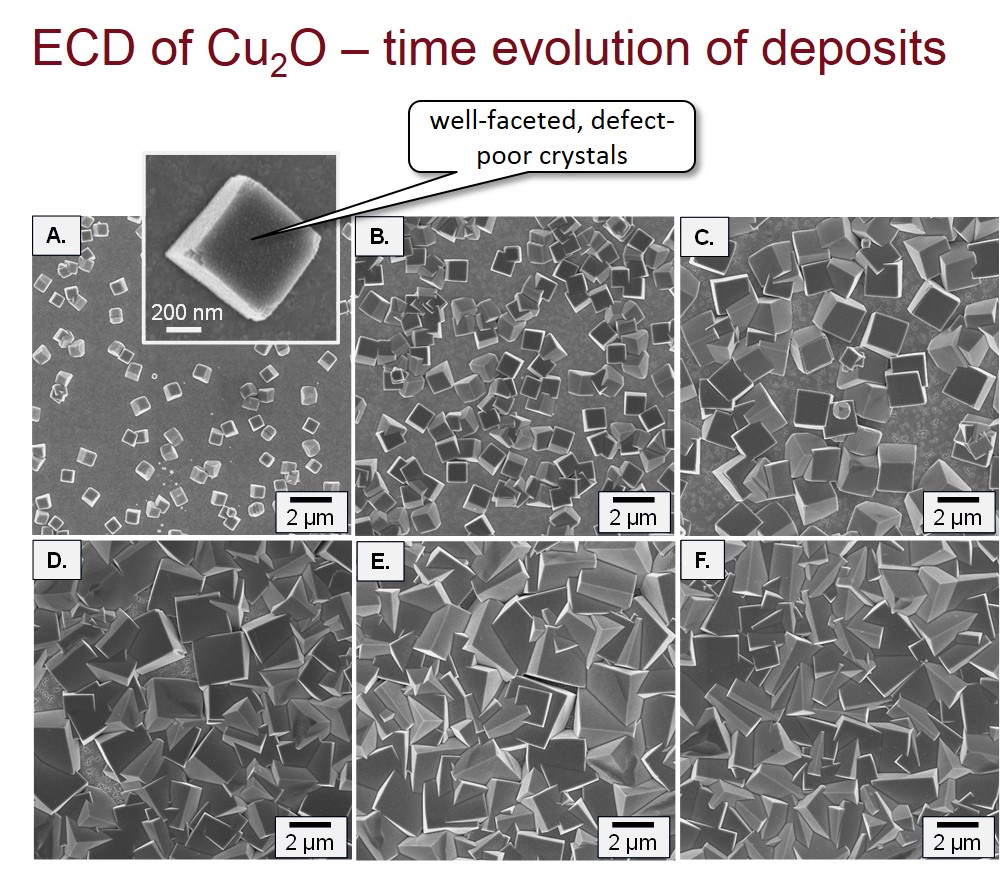
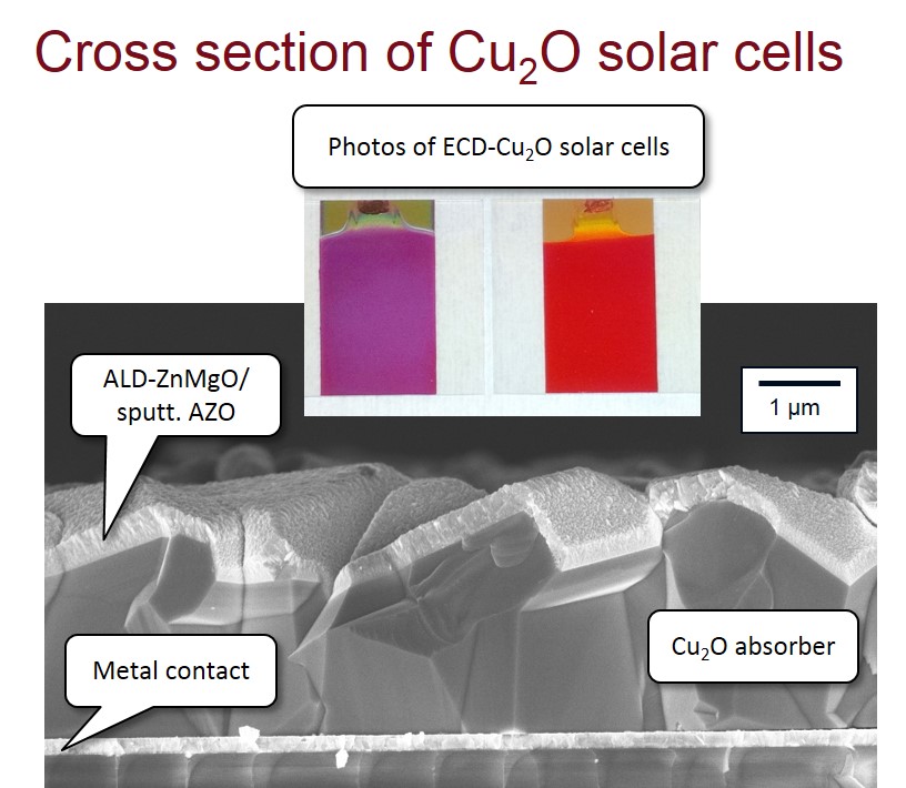
- The development of a precious-metal-free conductive substrate, based on Cr/ITO (chromium/indium-tin-oxide) that allowed for appropriate growth of the Cu2O absorber, giving rise to large crystals, compact absorber film (pinhole-free) and roughness profile that enhances the light absorption and the effective heterojunction surface.
- Development of ALD recipes for ZnO and Zn1-xMgxO thin films with different Mg content, giving rise to films with tunable bandgap and electron affinity that depend on the Mg content. This permited the improvement of the band alignment at the heterojunction with the absorber, which finally contributed to an enhancement of the photovoltaic performance of the cells.
- The development of layers of self-assembled molecules with different dipole moments on ZnO and Cu2O films, which permitted the modification of the work function of the oxide. Although these layers did not lead to an increase of PV performance, the obtained know-how can be applied to other optoelectronic devices to tune the device energetics.
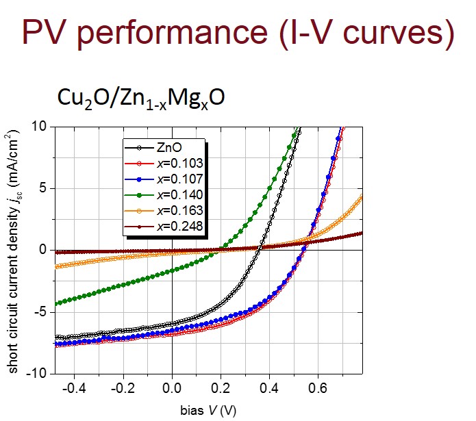
- Realization of Cu2O/ZnMgO solar cells with enhanced open circuit voltage, reaching more than 600 mV under AM1.5G solar illumination for the best cells. The highest measured power conversion efficiency was 1.7% using a ZnMgO layer (Mg doping below 10%) and an optimized Cu2O electrodeposition process. We have observed that with the appropriate Mg doping, the open circuit voltage is enhanced by more than 200 mV compared to ZnO.
As an outlook, CopperHEAD showed that it is possible to improve the PV performance of Cu2O-based cells by heterojunction engineering, reducing the defects and adjusting the energy band alignment. For this, high precision deposition methods, like atomic layer deposition, are valuable. The employment of mixed oxide compounds, such as the magnesium zinc oxide (ZnMgO), is a very promising approach to achieve band adjustment. This has been demonstrated in the project, for low Mg contents, through the reduction of the electron affinity of the film. The effect of PV performance increase was unfortunately reversed for larger Mg contents, evenif the electron affinity continued to decrease, most probably due to the introduction of deep-level defects in the ZnMgO layer.
Apart from ZnMgO, there are a number of other mixed oxides that could deliver more positive results when combined with the Cu2O absorber. Particularly promising candidates are the Ga2O3 and the ZnGeO, which have recently shown impressive results, the first combined with ECD-grown Cu2O (efficiency of 3.97%) and the second with thermally oxidized Cu2O (efficiency of 8.1%). The maximum achieved efficiency of 8.1% shows that all-oxide PV is a viable technology for future deployment, but more work has to be invested on finding the right heterojunction combination. So, an intensification of the efforts to study mixed oxide compounds is of paramount importance to enable commercialization of the all-oxide PV.
At the same time, tandem cells are increasingly appealing to harvest larger portions of light and increase the efficiency. Cu2O-based cells are particularly interesting as top cell in such tandem architectures. They can be combined with lower-bandgap inorganic absorbers (as bottom cells), such as CZTS or CIGS and even with certain hybrid perovskites. Research efforts towards this direction may further boost the field of abundant and low-cost PV.
Peer-reviewed articles
- Effect of thermal annealing in vacuum on the photovoltaic properties of electrodeposited Cu2O-absorber solar cell”, T. Dimopoulos, A. Peic, S. Abermann, E.J.W. List-Kratochvil, R. Resel, EPJ Photovoltaics5, 50301 (2014).
- All-oxide solar cells based on electrodeposited Cu2O absorber and atomic layer deposited ZnMgO on precious-metal-free electrode, J. Kaur, O. Bethge, N. Bansal, A. R. Wibowo, M. Bauch, R. Hamid, E. Bertagnolli, T. Dimopoulos, Solar Energy Materials and Solar Cells, 161,449 (2017).
Downloads

Dr. Theodoros Dimopoulos
Theodoros Dimopoulos erhielt seinen Master in Festkörperphysik von der Universität Athen und promovierte auf dem Gebiet der Spinelektronik an der Universität Louis Pasteur in Straßburg. Als Marie-Curie-Stipendiat in der Siemens Corporate Technology, lag sein Fokus auf Dünnschichttechnologie für magnetoresistive Sensoren und Speicher. Seit 2005 ist er Scientist/Senior Scientist am AIT und beschäftigt sich die letzten Jahren mit Materialien und Herstellungsverfahren für neuartige Photovoltaik-Technologien.
Steckbrief
-
Projektnummer84119
-
Koordinator
-
ProjektleitungTheodoros Dimopoulos, theodoros.dimopoulos@ait.ac.at
-
PartnerVienna University of Technology - Institute for Solid State Electronics
NanoTecCenter Weiz Forschungsgesellschaft mbH
-
FörderprogrammEnergieforschung (e!MISSION)
-
Dauer01.2013 - 12.2016
-
Budget40.000 €